Showing posts with label Basic electronics. Show all posts
Showing posts with label Basic electronics. Show all posts
Tuesday, 7 February 2012
Tuesday, 1 November 2011


Tuesday, 25 October 2011

Thursday, 13 October 2011
Basic Electronics Record Experiments List
- P-N Junction Diode Characteristics
- Zener Diode Characteristics
- Half Wave Rectifier
- Full Wave Rectifier
- Transistor CE Characteristics
- Transistor CE Amplifier
- Current Series Feedback Amplifier
- RC Phase Shift Oscillator
- FET Characteristics
Basic Electronics Assignment


These are few questions of our assignment. I'll upload remaining later.
Thursday, 22 September 2011
AIM: To calculate the frequency of the RC phase shift oscillator & to measure the phase angles at different RC sections.
THEORY:
RC-Phase shift Oscillator has a CE amplifier followed by three sections of RC phase shift feed back Networks the out put of the last stage is return to the input of the amplifier. The values of R and C are chosen such that the phase shift of each RC section is 60º.Thus The RC ladder network produces a total phase shift of 180º between its input and output voltage for the given frequencies. Since CE Amplifier produces 180 º phases shift the total phase shift from the base of the transistor around the circuit and back to the base will be exactly 360º or 0º. This satisfies the Barkhausen condition for sustaining oscillations and total loop gain of this circuit is greater than or equal to 1, this condition used to generate the sinusoidal oscillations.
The frequency of oscillations of RC-Phase Shift Oscillator is,
1
f = -----------
2pRC* √6
CIRCUIT DIAGRAM:

PROCEDURE:
1. Make the connection as per the circuit diagram as shown above.
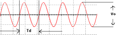
2. Observe the output signal and note down the output amplitude and time period (Td).
3. Calculate the frequency of oscillations theoretically and verify it practically (f=1/Td).
4. Calculate the phase shift at each RC section by measuring the time shifts (Tp) between the final waveform and the waveform at that section by using the below formula.
OBSERVATIONS:
THEORITICAL CALCULATIONS: R = 10KΩ, C = 0.001 μf
1
f = -------------- =
2pRC* √6
PRACTICAL CALCULATIONS:
Td =
1
f = -----
Td
Tp1
(1). θ 1= --------*3600 =
Td
Tp2
(2). θ 2 = ------- * 3600 =
Td
Tp3
(3). θ 3= ----------- *3600 =
Td
MODEL WAVE FORMS:
OUT PUT WAVE FORM :
OUT PUT WAVE FORM : θ = 600

OUT PUT WAVE FORM : θ = 1200

OUT PUT WAVE FORM : θ = 180

RESULT: The frequency of RC phase shift oscillator is calculated and the phase shift at different RC sections is noted.
VIVA QUESTIONS:
- What are the conditions of oscillations?
- Give the formula for frequency of oscillations?
- What is the total phase shift produce by the RC ladder network?
- Whether the oscillator is positive feedback or negative feedback?
- What are the types of oscillators?
- What is the gain of RC phase shift oscillator?
- What is the difference between damped oscillations undamped oscillations?
- What are the applications of RC oscillations?
- How many resistors and capacitors are used in RC phase shift network
- How the Barkhausen criterion is satisfied in RC phase shift oscillator
Thursday, 15 September 2011
15. CURRENT-SERIES FEEDBACK AMPLIFIER
AIM: To measure the voltage gain of current - series feed back amplifier.
APPARATUS: Transistor BC
Breadboard
Regulated Power Supply (0-30V,1A)
Function Generator
CRO(30 Mhz,dualtrace)
Resistors 33kΩ,3.3kΩ,330Ω,1.5kΩ,2.2k Ω,4.7k Ω, 1 k Ω.
Capacitors 10µF - 2Nos
100µF
CIRCUIT DIAGRAM:
THEORY:
When any increase in the output signal results into the input in such a way as to cause the decrease in the output signal, the amplifier is said to have negative feedback.
The advantages of providing negative feedback are that the transfer gain of the amplifier with feedback can be stablised against varations in the hybrid parameteresof the transistor or the parameters of the other active devices used in the circuit. The most advantage of the negative feedback is that by propere use of this, there is significant improvement in the frequency respponse and in the linearity of the operation of the amplifier.This disadvantage of the negative feedback is that the voltage gain is decreased.
In Current-Series Feedback, the input impedance and the output impedance are increased.Noise and distortionsare reduced cosiderably.
PROCEDURE:
1. Connections are made as per circuit diagram.
2. Keep the input voltage constant at 20mV peak-peak and 1kHz frequency.For different values of load resistance, note down the output voltage and calculate the gain by using the expression
Av = 20log(V0 / Vi ) dB
3. Remove the emitter bypass capacitor and repeat STEP 2.And observe the effect of feedback on the gain of the amplifier.
4. For plotting the frquency the input voltage is kept constant at 20mV peak-peak and the frequency is varied from 100Hz to 1MHz.
5. Note down the value of output voltage for each frequency. All the readings are tabulated and the voltage gain in dB is calculated by using expression Av = 20log (V0 / Vi ) dB
6. A graph is drawn by takung frquency on X-axis and gain on Y-axis on semi log graph sheet
7. The Bandwidth of the amplifier is calculated from the graph using the expression Bandwidth B.W = f2 – f1.
Where f1 is lower cutt off frequency of CE amplifier
f 2 is upper cutt off frequency of CE amplifier
8. The gain-bandwidth product of the amplifier is calculated by using the expression
Gain-Bandwidth Product = 3-dB midband gain X Bandwidth.
OBSERVATIONS:
Voltage Gain: Vi = 20 mV
S.NO | Output Voltage (Vo) with feedback | Output Voltage (Vo) without feedback | Gain(dB) with feedback | Gain(dB) without feedback |
Frquency Response:
S.NO | Frequency (Hz) | Output Voltage (Vo) | Gain A = Vo/Vi | Gain in dB 20log(Vo/Vi) |
MODEL WAVEFORM:
Frequency response
PRECAUTIONS:
1. While taking the observations for the frequency response , the input voltage must be maintained constant at 20mV.
2. The frequency should be slowly increased in steps.
3. The three terminals of the transistor should be carefully identified.
4. All the connections should be correct.
RESULT:
The effect of negative feedback (Current-Series Feedback ) on the amplifier is observed. The voltage gain and frquency response of the amplifier are obtained.Also gain-bandwidth product of the amplifier is calculated.
VIVA QUESTIONS
1. What is the effect of Current-Series Feedback amplifier on the input inmpedance of the amplifier?
2. What is the effect of negative feedback on the Bandwidth of an amplifier?
3. State the reason for the usage of negative feedback in an amplifier?
4. What are the fundamental assumptions that are made in studying feedback amplifiers?
5. What are the advantages of providing negative feedback amplifier?
6. What are the ideal characteristics of a voltage amplifier?\
7. Draw the circuit for the current series feedback?
8. What is the other name for current series feedback amplifier?
9. What is the formula for input resistance of a current series feedback?
10. What is the formula for output resistance of a current series feedback?
Subscribe to:
Comments (Atom)